Display Port 1.4 link Training 过程
DP link traing 及DP问题的一点总结
最近遇到2个DP link training失败的问题,问题解决后本想写一篇Link Training的总结,发现自己可写的东西比较少,现将网络上比较好的笔记总结如下,供以后遇到问题的同学参考。
目录
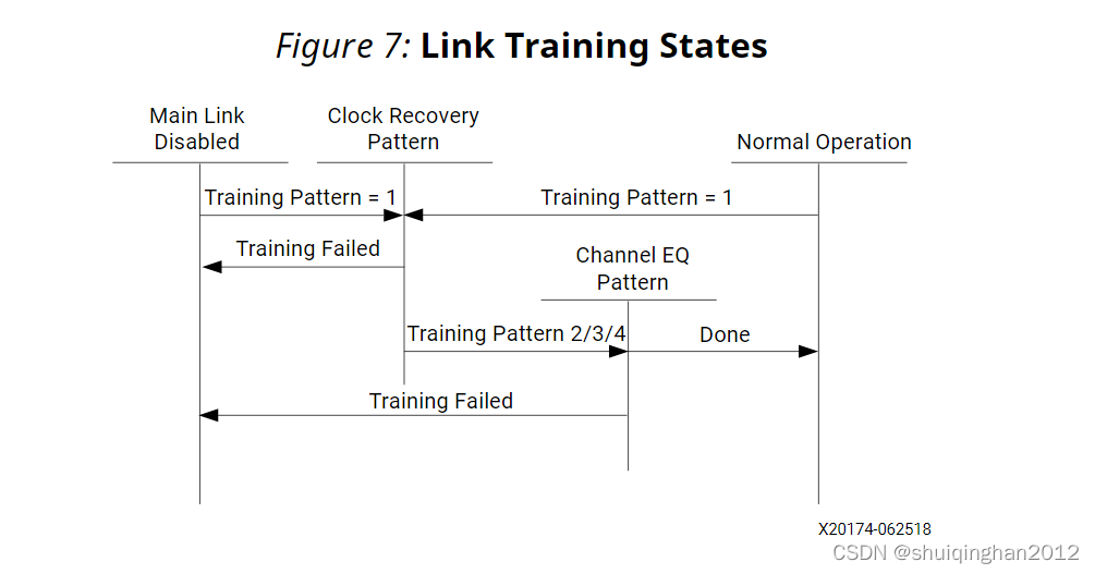
4.3.5. DisplayPort Link Training Flow
如下为个人笔记
DP link training 重要的资料来源
分别为Intel DP 用户指导,xlinx DP 用户指导,协议手册及协议分析仪的log分析,链接如下
https://www.xilinx.com/support/documents/ip_documentation/v_dp_txss1/v3_1/pg299-v-dp-txss1.pdf
Ref Chapter 5 Link Training

ref intel
4.3.5. DisplayPort Link Training Flow
4.3.5. DisplayPort Link Training Flow
Upon Hot Plug detection, the DisplayPort source configures the link through link training.
The DisplayPort source device accesses the sink’s DPCD register block through the AUX channel to determine the sink’s capability and status and initiate the Link Training command.
The sequence below describes the Link Training flow after HPD assertion:
- The DisplayPort source reads the DPCD Capabilities fields offset 0x00000 – 0x0000D to determine the sink device’s capability.
- The source writes to the Link Configuration field offset 0x00100 – 0x00101 to configure the Link Bandwidth and Lane Count according to the sink device’s requirements.
After Link Configuration, the source initiates Link Training Pattern Sequence 1.
- The source writes to offset 0x00102 to select Training Pattern 1 and Disable Scrambling. The source sends Training Pattern 1 through the Main Link at the same time.
- The source writes to offset 0x00103 – 0x00106 to configure the Link Training Control for every lane.
- The source reads from offset 0x0000E for TRAINING_AUX_RD_INTERVAL value.
- The source waits for a period of time specified in TRAINING_AUX_RD_INTERVAL before it reads the Link Status (0x00202 – 0x00207) from the sink device.
- If the clock recovery core (CR_DONE) fails in one or more lanes:
- The source checks for the Link Driver setting adjust request (0x00206 – 0x00207) and responds accordingly.
- In the same Link Driver setting, if the source has already repeated Training Pattern Sequence 1 for 5 times, the source will lower the Link Bandwidth (from HBR2 to HBR to RBR) in offset 0x00100 and starts back at Step 1.
- If the Link Bandwidth is already in the lowest rate (RBR), then Link Training fails.
For Link Training Pattern Sequence 2:
- The source writes to offset 0x00102 to select Training Pattern 2 and Disable Scrambling. The source sends Training Pattern 2 through the Main Link at the same time.
- The source writes to offset 0x00103 – 0x00106 to configure the Link Training Control for every lane.
- The source reads from offset 0x0000E for TRAINING_AUX_RD_INTERVAL value.
- The source waits for a period of time specified in TRAINING_AUX_RD_INTERVAL before it reads the Link Status (0x00202 – 0x00207) from the sink device.
- If CR_DONE (0x00202) fails in one or more lanes, abort Training Pattern Sequence 2, and restart Training Pattern Sequence 1.
- If CR_DONE passes all lanes, check if the following operations fail or pass:
- CHANNEL_EQ_DONE
- SYMBOL_LOCKED
- INTERLANE_ALIGN_DONE
- If CHANNEL_EQ_DONE, SYMBOL_LOCKED or INTERLANE_ALIGN_DONE fails in one or more lanes:
- The source checks for the Link Driver setting adjust request (0x00206 – 0x00207) and responds accordingly.
- In the same Link Driver setting, if the source has already repeated Training Pattern Sequence 2 for 5 times, the source will lower the Link Bandwidth (from HBR2 to HBR to RBR) in offset 0x00100, aborts Training Pattern Sequence 2, and restarts Link Training Pattern Sequence 1.
- If the Link Bandwidth is already in the lowest rate (RBR), then Link Training fails.
- If Training Pattern Sequence 2 passes, then Link Training completes.
- The source writes to offset 0x00102 to disable Link Training.
Note: If both DisplayPort source and sink support HBR2, replace Training Pattern Sequence 2 with Training Pattern Sequence 3.
时钟恢复总结
DisplayPort--Link training之Clock Recovery (CR)_dp link training_垮掉一代的博客-CSDN博客
Ref DP协议规范3.6.6
Ref:协议分析仪分析过程及文档
网络上很多截图都来源于此文档
Webinar: DisplayPort Compliance Test Overview Part Two: Protocol
如下这位仁兄的总结很好,里面包含了很重要的几张图
DP1.4协议 关键特性总结_csdn1013的博客-CSDN博客
个人根据自己的理解以及遇到的问题,再总结下关键点;
一.连接框图及主要信号


信号按类别分4种
1. main link
Unidirectional, high-bandwidth channel used to transport
video, audio, metadata and protocol control elements.
Main Link 1, 2 or 4 Lane Configurations.
Main Link 4 link rates:
1.62Gbps (Reduced Bit Rate)
2.7Gbps (High Bit Rate)
5.4Gbps (High Bit Rate 2)
8.1Gbps (High Bit Rate 3)
No clock channel. Sink recovers clock using link transitions.
单向高带宽传输通道,用来传输视频,音频,元数据,和协议控制命令等,注:没有单独的时钟通路,因此sink端需要时钟数据恢复电路CDR,DP也是标准serdes的电路。
在电路图上为差分4组lane 阻抗100ohm,AC 耦合

2.AUX Channel
Aux Channel: Bidirectional, half duplex channel at 1Mbps. Link Training, DSC and FEC Configuration, DPCD Register status, HDCP authentication & EDID exchange.
AUX辅助通道为:1Mbps的双向半双工信道。链路训练(LT/Link Training)、DSC和FEC配置、DPCD寄存器状态、HDCP认证和EDID交换。
电路上为AUX_P/N 差分 100ohm阻抗,AC耦合
电路注意两个点
1.AUX_N需做上拉,AUX_P做下拉
2.TX Source端上下拉为100K 常用
3.RX Sink端上下拉为1M 常用

3.HPD hot Pulg
Connection Detection.
Interrupt mechanism for link failures.
连接检测。
链路故障的中断机制。

HPD de-bounce time:
- DPTX are recommended to implement de-bouncing of the HPD signal on an external connection
- A period of 100 ms is recommended for the detection of an HPD connect event.
比如 the event, “HPD High”, is confirmed only after HPD has been asserted continuously for 100 ms.

原文链接:https://blog.csdn.net/CSDN1013/article/details/106992157
4.Power

二. Link traing 重要的参数
DPCD中重要的配置参数
TP1 TP2
CR_DONE
EQ_DONE
SYMBOL_LOCKED

如下是link ok的状态,0x9977,后4位 0111,其中后3位全为1对应寄存器描述如上,已经全部done
LINK_BW_SET (0x400) status in DPCD = 0x14
LANE_COUNT_SET (0x404) status in DPCD = 0x4
LANE0_1_STATUS (0x043C) in DPCD = 0x9977
LANE2_3_STATUS (0x440) in DPCD = 0x9977
link fail的状态如下,后4位全部为0
LINK_BW_SET (0x400) status in DPCD = 0x6
LANE_COUNT_SET (0x404) status in DPCD = 0x4LANE0_1_STATUS (0x043C) in DPCD = 0x3300
LANE2_3_STATUS (0x440) in DPCD = 0x3300SYM_ERR_CNT01 (0x448) = 0x80008000
SYM_ERR_CNT23 (0x44C) = 0x80008000
其中这个参数TRAINING_AUX_RD_INTERVAL也很重要,决定了link的间隔时间
Link training的关键指标: CR和EQ
Clock Recovery (CR): Link training begins with the Clock Recovery (CR) sequence. 时钟锁定和差分电压Vpp设置. Locks the receiver CR (clock recovery) PLL when successful.
Channel Equalization (EQ):Symbol-Lock & Inter-lane Alignment and Pre-emphasis setting.
注意: Training发生在读RX DPCD,EDID之后。
Link training for DPCD:
CR time out: 100us
EQ time out: Optional. 400us, 4ms, 8ms, 12ms,16ms
在Fast training中,没有AUX transaction
————————————————
版权声明:本文为CSDN博主「csdn1013」的原创文章,遵循CC 4.0 BY-SA版权协议,转载请附上原文出处链接及本声明。
原文链接:https://blog.csdn.net/CSDN1013/article/details/106992157
对应DPCD 00E寄存器
/* 0x0000E: TRAIN_AUX_RD_INTERVAL */

/* *** Definitions for DP 1.4 :: DPCD parameters. */
#define XDP_DPCD_TRAIN_AUX_RD_INT_MASK				0x7F
/* *** DP 1.4 :: DPCD definitions end. */

#define XDP_DPCD_TRAIN_AUX_RD_INT_100_400US			0x00
#define XDP_DPCD_TRAIN_AUX_RD_INT_4MS				0x01
#define XDP_DPCD_TRAIN_AUX_RD_INT_8MS				0x02
#define XDP_DPCD_TRAIN_AUX_RD_INT_12MS				0x03
#define XDP_DPCD_TRAIN_AUX_RD_INT_16MS				0x04
这个参数要从RX端的DPCD中配置中读取然后配置的TX端,主要这部分的软件操作。
三.Link training 失败经验
器件异常,I2C操作失败,时序不对,TX和RX配置不同,都会导致失败,
要抓log具体分析,尤其是TP1之前的失败大概率和硬件有关,如能进入到TP2,大概率是软件配置问题。
更多推荐
 已为社区贡献1条内容


所有评论(0)